A patented paste, CuB+, uses ceramic-copper composites as DCB hybrid technologies to provide enhanced electro-thermal and mechanical performance compared to standard DCB technology.
By Christian Winkler and Munsoo Han, Consultants, Global BA GmbH
DCB substrates with AMB performance – at DCB cost?
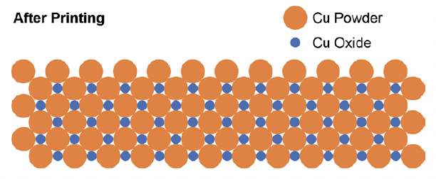
CuB+ paste can be applied as a homogeneously-oxidized copper powder to all common substrate types, including Al2O3, ZTA, AlN and Si3N4. Used this way, CuB+ increases the mechanical performance (thermal cycling) of standard DCB substrates, making it directly comparable with AMB substrates.

Figure 1: Shows the applied copper paste after screen printing. The paste may also be applied with other common coating techniques such as dispersion or inkjet.
As well, manufacturing cost is significantly reduced since the use of expensive AMB active solder is avoided and there is no requirement for vacuum and second etching processes.

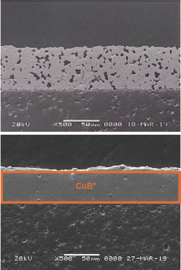
Figure 2: Conventional copper printed thick layer solution.
Figure 3: New and non-porous CuB+ connection technology.
Partial discharge-free?
The homogeneous coating and pore-free connection enable the achievement of partial discharge-free DCB substrates for high voltage over 1,7kV applications as well.
Power and logic on one device?
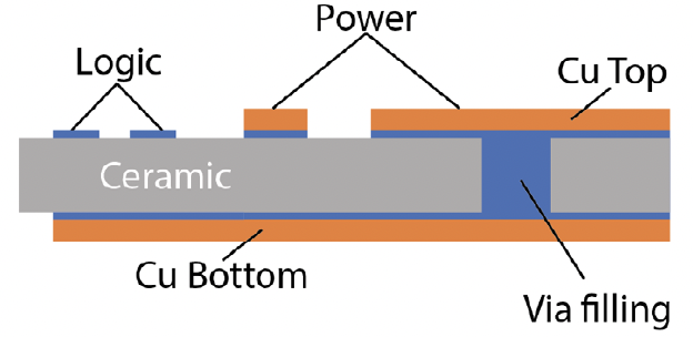
The freedom offered by the coating technology allows for delivery of power and logic on a substrate as a DCB hybrid solution. Hermetically- sealed through-connections for high frequency or low inductance requirements are also easy to implement.

Figure 4: DCB substrate with Integrated power and logic on one device for low-cost and lowinductance power module designs with via filling.
Warpage control and hysteresis behaviour on DCBs?
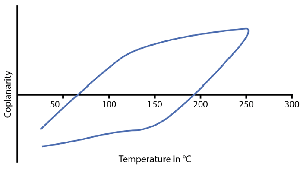
The use of selective copper paste on the upper surface of the substrate can reduce warpage by reducing the bi-metal effect that arises from the relative deficiency of copper with respect to the bottom surface.

Figure 5: The warpaging behaviour during power module soldering, return ideally back to the original condition.
CuB+: a clear booster for DCB substrates and power modules
• No use of heavy metal e.g. lead, cadmium (RoHS conformant).
• High purity copper layer (> 99.0%).
• Partial discharge-free (< 10pC).
• Excellent electrical and thermal properties, equal to copper.
• Applicable to Al2O3, ZTA, AlN and Si3N4 ceramics.
• Excellent wire-bonding and soldering / sintering properties.
• A wide variety of applications.
• Lower process cost than AMB.
• Zero-void technology by DCB-bonding.
• Available for licensing or technology transfer


